Home / Instruments / Field Emission Scanning Electron Microscope (FESEM)
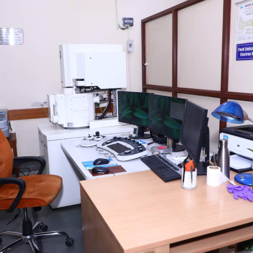
Field Emission Scanning Electron Microscope (FESEM)
You need a USIC account to book this instrument —
log in or
create a free account.
Requisition forms
Please download the requisition form, fill it in, sign it, and upload the filled copy with your booking. This requisition form is provided by the USIC office for this instrument.
Process: submit booking → in-charge approval → pay on the DU fee portal → upload Order ID + receipt → measurement confirmed. See the payment flowchart and user guidelines.
About this instrument
Model- Gemini SEM 500
FEATURES
- Materials Science: Microstructure analysis, fracture analysis, and compositional
studies.
- Nanotechnology: High-resolution imaging of nanostructures and thin films.
- Life Sciences: Imaging of biological specimens.
- Industry: Battery and device characterization.
- Energy-Dispersive X-ray Spectroscopy (EDS)
Octane Elect Super: 70 mm² active area, Silicon Nitride (Si₃N₄) Window: Offers
superior transmission compared to polymer windows, enhancing sensitivity to light
elements like carbon, nitrogen, and oxygen.
SPECIFICATION
- Scale: 20 nm to 100 um
- Accelerating Voltage Range: 0.02 to 30 kV
- Magnification Range: 50× to 2,000,000×
- Probe Current: 3 pA to 20 nuA (up to 100 nA optional)
- Working Distance: 0.1 mm to 50 m
Detector- In-lens detector and backscattered detector and EDS detector
SAMPLE – Powder and thin films