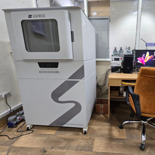
Atomic Force Microscope (AFM)
Requisition forms
Please download the requisition form, fill it in, sign it, and upload the filled copy with your booking. This requisition form is provided by the USIC office for this instrument.
Process: submit booking → in-charge approval → pay on the DU fee portal → upload Order ID + receipt → measurement confirmed. See the payment flowchart and user guidelines.
About this instrument
The “Surfmera VEGA-PROXIMA AFM” is a fully automated atomic force microscope with ultimate stability and resolution for industrial and research applications. It supports large samples up to 200 × 200 mm and offers high-accuracy positioning, low noise, and advanced AFM mode in a single system.
1. Electronics & Software
1.1. Signal Processing:
- Up to 24 scan channels
- 512 Mb buffer; multiple high-speed FPGAs & DSP processors
1.2. Lock-in & Signal Generation:
- 2 × analog lock-in amplifiers
- 3 × digital lock-in amplifiers (supporting multifrequency modes)
- 6 × 32-bit digital generators with advanced modulation options
1.3. Voltage Supplies:
- ±10 V for independent tip and sample bias
- ±150 V (optional) for extended bias experiments
1.4. Software & Automation:
- Autofocus (laser/cantilever/sample), automated multiple area scanning
- Optical + AFM image overlay and panoramic optical view
2. Scanner & Positioning
2.1 Scanner (tip-scanning):
- Type: Tube scanner with closed-loop sensors (XYZ)
- Scan range (standard): 100 × 100 × 10 µm (XYZ)
- Closed-loop: XYZ for all directions
- Drive electronics noise: < 5 µV/√Hz
2.2 Sample Positioning (Motorized Stage):
- Moving range: 200 × 200 mm in XY, 30 mm in Z
- Positioning accuracy: ~1 µm (XY) and 0.2 µm (Z)
- Thermal drift (stage): < 0.2 nm/min
- Positioning speed: ~8 mm/s in XY
- Navigation: Automated by video image or user-defined scanning scenario
3. Core AFM Modes
3.1. Contact & Static Modes
- Contact AFM – Topography: Surface height mapping in direct contact.
- Lateral Force Microscopy (LFM): Maps friction or lateral forces on surface.
- Force Modulation: Mechanical property contrast via modulated contact force.
- Spreading Resistance Imaging (SRI): Conductivity/resistance contrast in
contact. - Piezoresponse Force Microscopy (PFM): Mapping ferroelectric domains and
domain boundaries
3.2. Amplitude Modulation & Dynamic Modes
- Amplitude Modulation (AM) AFM – Topography: Tapping (intermittent
contact) imaging. - Phase Imaging: Tracks cantilever phase shift for material contrast.
- Feedback Channel Scanning: Maps feedback signal for improved detail.
3.3. Electrical & Electrostatic Modes
- Kelvin Probe Force Microscopy (KPFM)
- Single- and two-pass
- Amplitude & phase modulation modes
3.4. Electrostatic Force Microscopy (EFM)
- Single- and two-pass
- Amplitude & frequency modulation
3.5. Scanning Capacitance Force Microscopy (SCFM)
- Single- and two-pass
- dC/dZ and dC/dV capacitance imaging
These modes allow mapping of surface potential, charge distributions, and dielectric properties at the nanoscale.
3.6. Magnetic Force Microscopy (MFM)
- Two-pass lift modes
- Frame lift DC/AC magnetic contrast imaging
Used for magnetic domain structures, thin magnetic films, and data storage materials.
3.7. Spectroscopy & Force Curves
- Force–Distance Spectroscopy – Force curves vs separation
- Amplitude–Distance & Phase–Distance Spectroscopy
- I(V) and I(Z) – Current vs bias and height curves
3. Nanolithography
- Voltage-driven lithography
- Current-driven lithography
- Force-driven lithography
Supports patterning and modification of surfaces at the nanoscale.
4. Sample Requirement: The sample must be a completely dry, thin film synthesized using
an appropriate scientific method.